Electronics Design
Redraw the echo hello-world board; add a button and an LED; mill, stuff, and test it.
Assignment
-
Group project :
Using the test equipment in your lab to observe the operation of a microcontroller circuit board. Which can be found here.
-
Individual project:
- Redraw the echo hello-world board
- Adding (at least) a button and LED (with current-limiting resistor)
- Check the design rules, make it, and test it
What I made this week
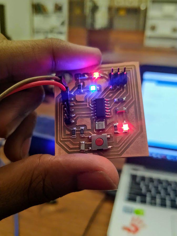
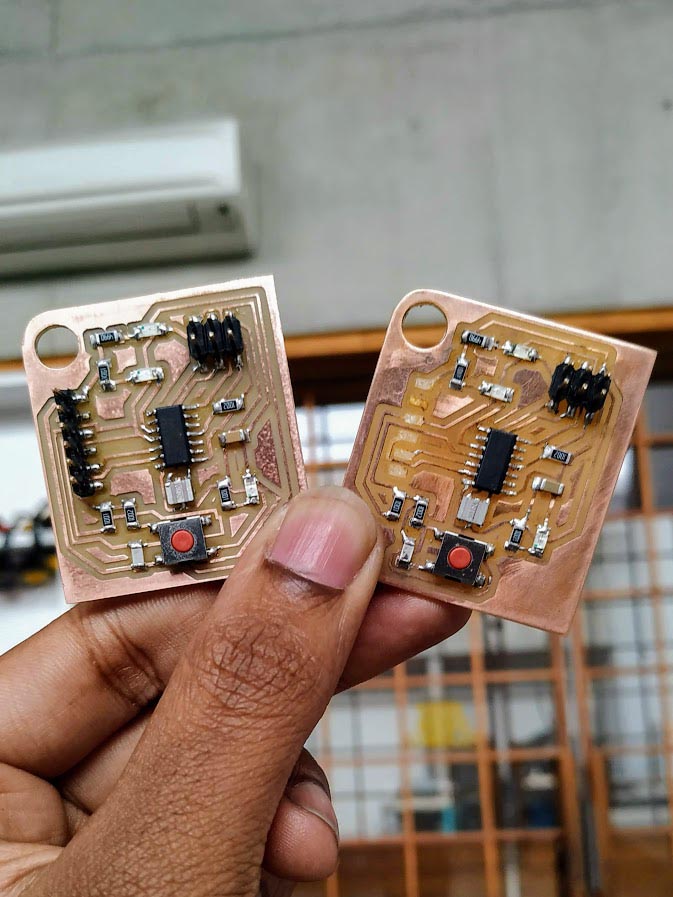
1. Electronics Basics
Circuits and the Flow of Current
Before beginning drawing or designing my own circuit I need to explain how a circuit works and how the flow of current works in a circuit. I found this tutorial by sparkfun to be the best explanation of what is a circuit and how it works. For Voltage and current, this tutorial, again by sparkfun, was very helpful.
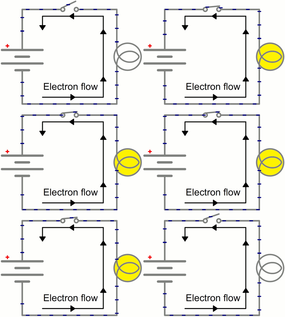
Link
- What is a Circuit?- by Sparkfun Electronisc
- Voltage, Current, Resistance, and Ohm’s Law- by Sparkfun Electronics
Components: Active vs Passive components
To make circuits, we’ll need components. All electronics components can be divided into two basic groups.
-
Active Components:
An active device is any type of circuit component with the ability to electrically control electron flow (electricity controlling electricity). In order for a circuit to be properly called electronic, it must contain at least one active device
-
Passive Components
Components incapable of controlling current by means of another electrical signal are called passive devices. Resistors, capacitors, inductors, transformers, and even diodes are all considered passive devices
This Infographic by Codrey illustrates Active vs Passive Electronics devices/components.
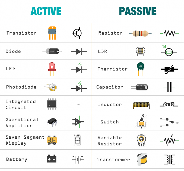
Learning what each of these components do is a long and tedious process. But to get started, I found this tutorial by Sparkfun Electronics very helpful.
As for my own introduction to electronics back in 2012, I read Robotics By Beginners,by David Cook which was available at my local library.
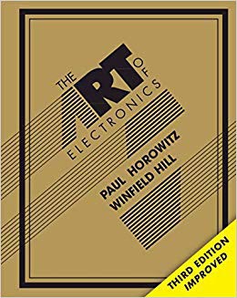
The Art of Electronics is a really good one, which I wish I had read earlier.

Link
Circuit Design Software
To make life easier for us electronics enthusiasts, there is a myriad of circuit design softwares. Some of them are free, some of them have limited capabilities , while some are industry grade, like Altium, which can cost upto 7,500$ for a one year license.
Workflow:
Despite of having many electronics design softwares, most of them work on the same basic workflow.
- First you make a Schematic of your circuit
- Then you pick appropriate parts for your schematic
- Then you make a PCB for the circuit you designed with your designated parts
Circuit Design Software Jargon
-
Schematic:
A Schematic is a wire diagram of your circuit. A free-hand drawing like this can also be called a schematic
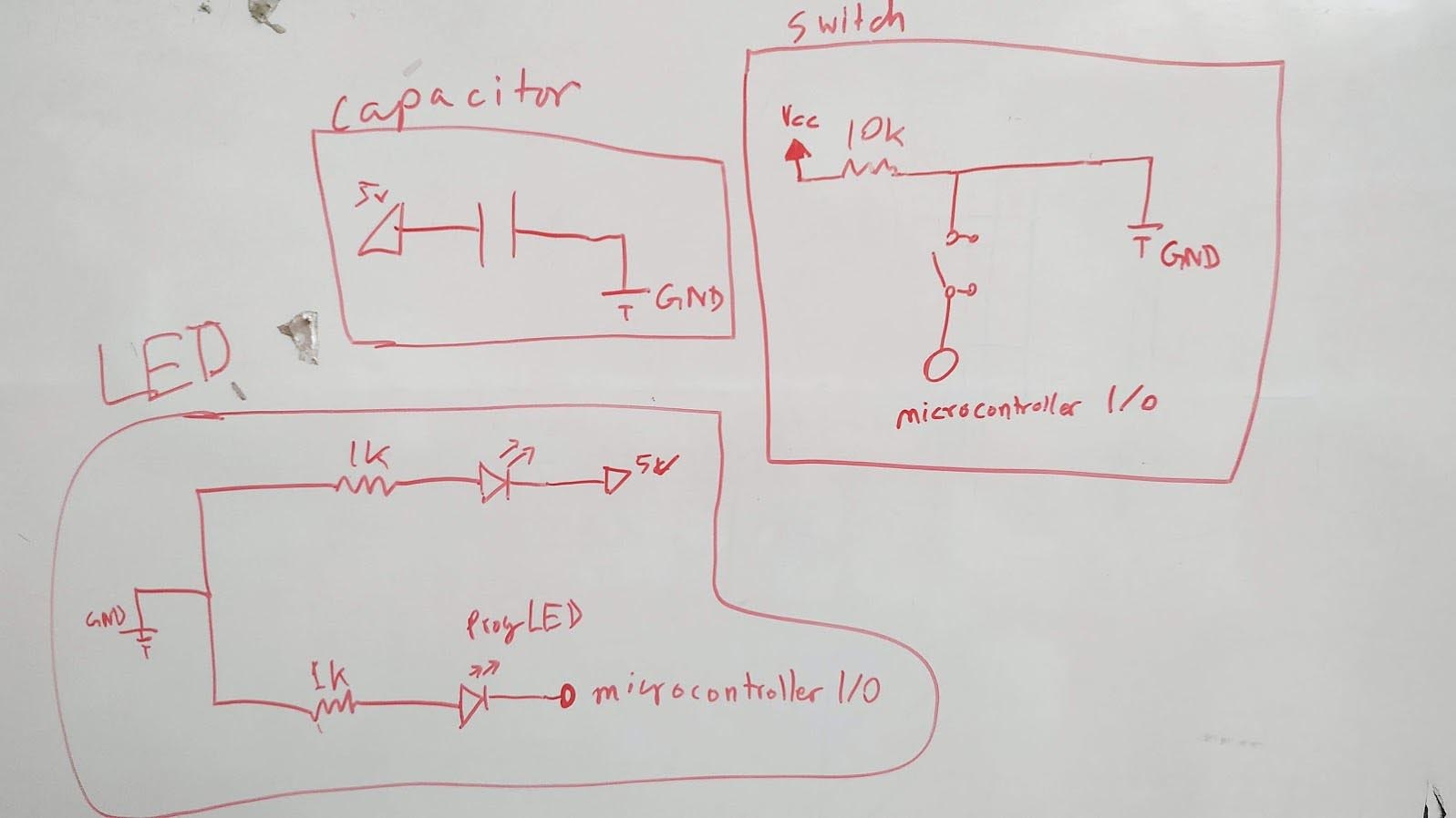
Freehand schematic of the parts I wanted to add to my hello echo board -
Component Package & Footprints
Electronics components come in different sizes and shapes. The integral part inside though, is VERY VERY small. Which means, that the same IC can come in a tiny package, or it might come in a big package with better thermal properties. As for example, the brains of this 8 pin through hole component can be seen in this image, which is not even half of the total package size.
This method of taking out the externals of an IC to reveal it’s inner workings is called ‘Decapping’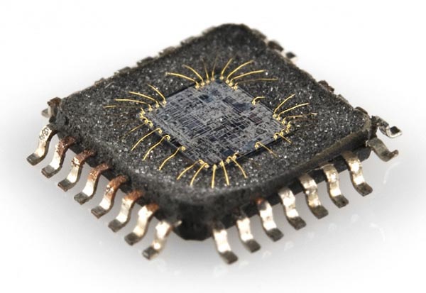
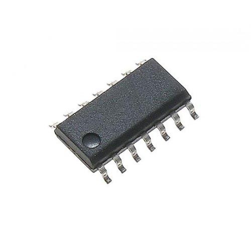
Decapping an IC- illustration by SparkFun For ease of use electronic components usually come in some generalized package dimensions. As for example, the ATTINY44 we work with at our lab comes in the SOIC-14 package. These packages make it very convinient for the components to be used in Electronics Design softwares.
A component footprint on the other hand is the design/placement of a component on copper on a circuit board. It is the same size as the package of the component and sometimes, for rare components you might have to make your own component footprints.
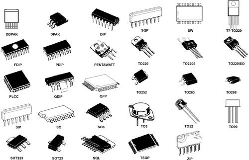
Various Package Types- Illustration by Sparkfun Links
-
Component Library
A component Library is a a collection of the pin mapping and the PCB footprints of an electronic component. This makes designing PCBs an easy process for us all. Component Libraries will vary for different design softwares. A good source of component libraries for KiCAD and Eagle is SnapEDA.
Links
-
Wires and Terminals
As the name suggests, wires are just plain wires. They will connect one point with another in a schematic. A terminal is a junction of wires, where they intersect.
-
Traces
Traces are the manifestation of the wires in a PCB made on the copper layer of a PCB. Trace width can vary according to the design but they too have certain standard values. Traces are generally calculated in Mils or Thous.
-
Routing
The process of connecting these traces is called routing. It is done according to the schematic and can be done automatically in some design softwares.
-
Layers
Layers in a PCB is the biggest factor contributing to the expense and ease of manufacturing. Usually we will be working with Single and Double layered boards. It gets much more complex and expensive in adding more boards. More on PCBs and layers can be found here.
Links
2. Disecting Neil’s Hello Echo Board
Here is all I could find about Neil’s Hello Echo board.
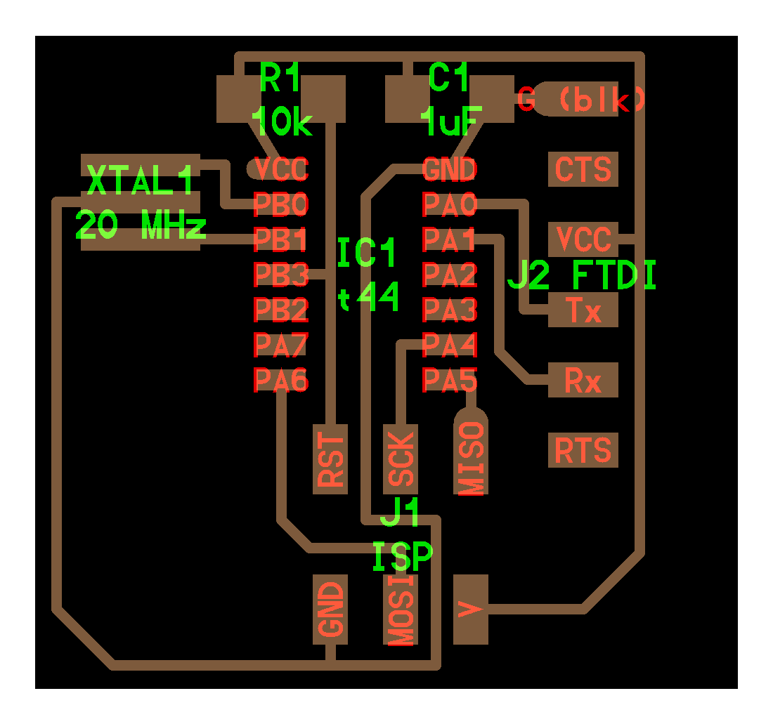
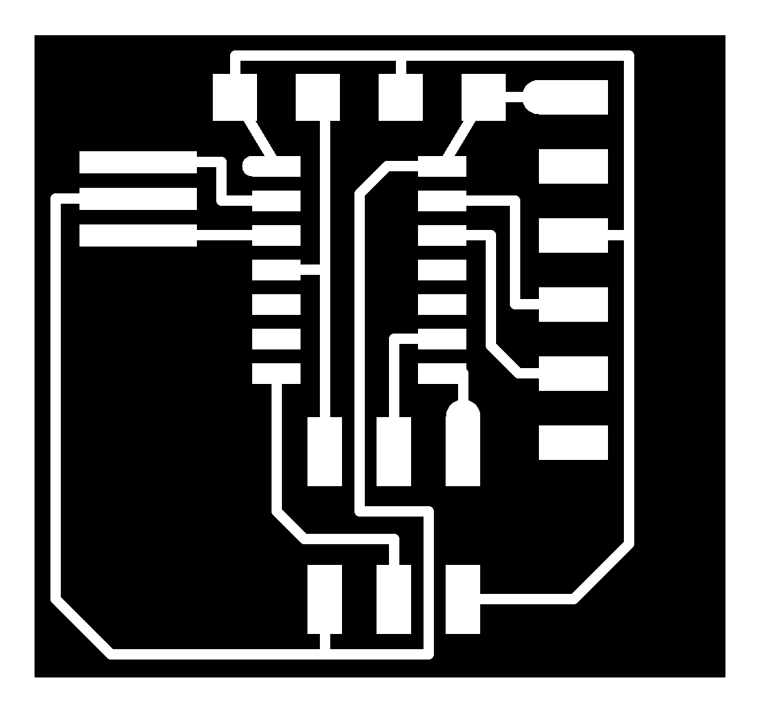
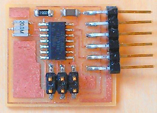
> Components on the original Hello Echo Board
ATTiny44:
The board is centered around a ATTiny44 microcontroller.
The Specs for it can be found on microchip’s website.
| Name | Value |
|---|---|
| Program Memory Type | Flash |
| Program Memory Size (KB) | 4 |
| CPU Speed (MIPS/DMIPS) | 20 |
| SRAM Bytes | 256 |
| Data EEPROM/HEF (bytes) | 256 |
| Digital Communication Peripherals | 1-SPI, 1-I2C |
| Capture/Compare/PWM Peripherals | 1 Input Capture, 1 CCP, 4PWM |
| Timers | 1 x 8-bit, 1 x 16-bit |
| Number of Comparators | 1 |
| Temperature Range (C) | -40 to 85 |
| Operating Voltage Range (V) | 1.8 to 5.5 |
| Pin Count | 14 |
10k Pullup Resistor
There is a 10k Pullup Resistor for the reset pin. As the name suggests, this resistor pulls the voltage up to 5v. More on Pullup resistors can be found here. We are using standard 1206 package resistors for the Fab Academy.
20Mhz resonator
Resonators function like crystals but stick closer to their specified frequency over a full temperature range. These resonators are +/-0.5% or better from -20C-+80C. These resonators have built-in load capacitors so no external caps are needed.
1uF Power Capacitor
The purpose of this capacitor is to smooth out the power supply for the microcontroller.
6Pin ISP Programmer Connector
The 6pin ISP programmer connector is used to program the ATTINY44. If you look back, the FABISP also has an identical connector.
FTDI Connector
The FTDI connector is for communication with a FTDI USB Serial chip. Luckily I have one, but I assume that we are going to make one in the communications week.
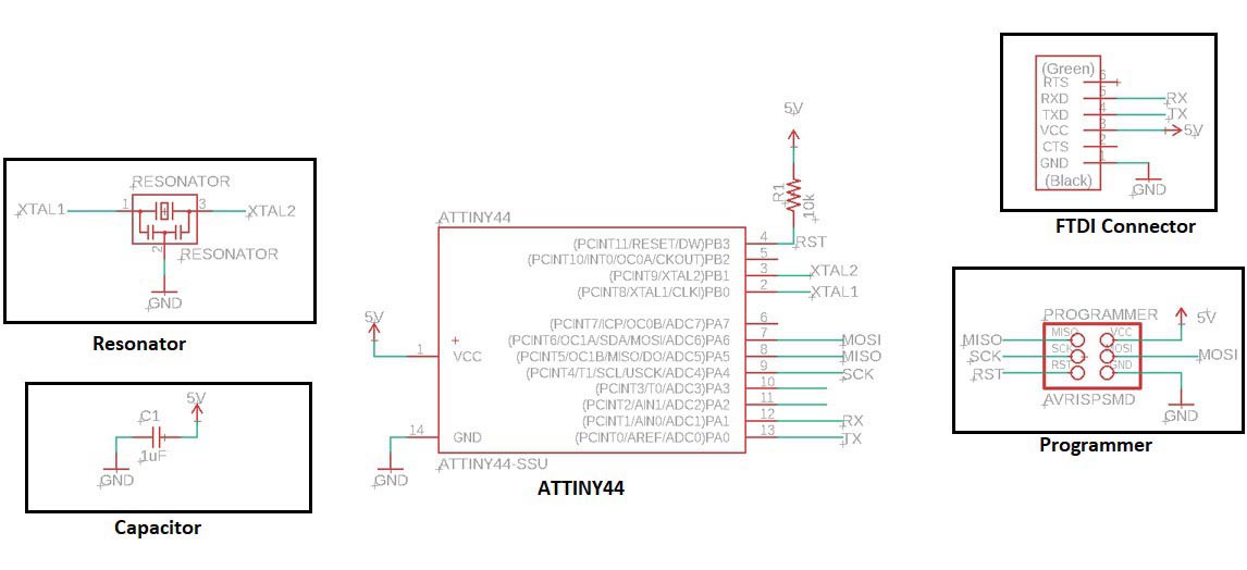
> Schematic of the original hello echo board
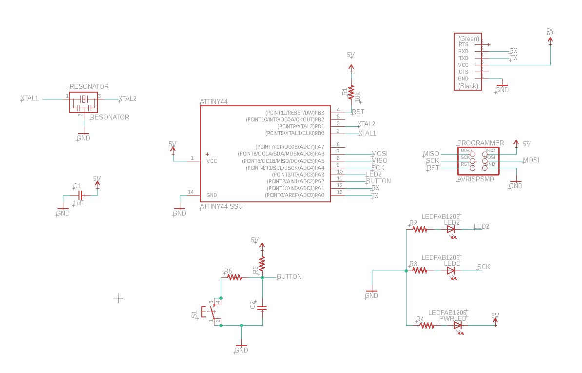
After analyzing the circuit, this is the schematic I came up with.
> Checking the hello echo firmware by Neil
I was not sure about the Tx and Rx pins so I had a look at Neil’s firmware code for the hello Echo board. Which can be found here. Download as .ino And I found PA0 was defined the serial pin in
PA1 was defined as serial pin out.
3. Planning out my Circuit
So I decided not to change the basics of the Hello Echo board, because I want my board to be compatible with Neil’s firmware to check the Hello Echo. But, I would like to add some components to it and create my own board based on this schematic.
The components that I decided to add were;
- A pusbutton
- 2 programmable LEDs
- One Power LED
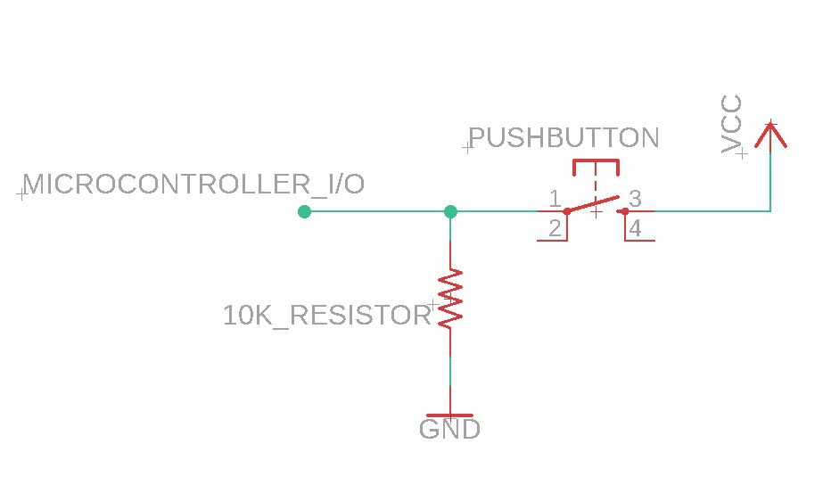
>Adding the Pushbutton:
A pushbutton is a tactile switch that connects two of its pins when the button is pressed. We can easily take and input on a microcontroller pin using a pull down resistor and a pushbutton. The logic is that the input pin will be pulled down using a high value resistor, which will always give a LOW on that I/O pin.
But! when the button is pressed, it will get connected to 5V and give a HIGH reading.
This is the easiest way to add a pushbutton to a circuit. But it has a problem. And it is called bouncing.
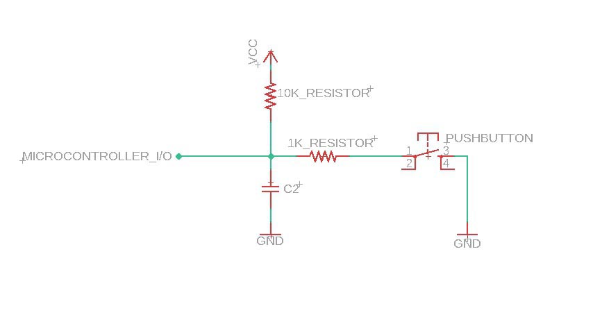
I usually use a debouncing technique that utilizes a capacitor and resistors. More on this topic can be found here.
Links
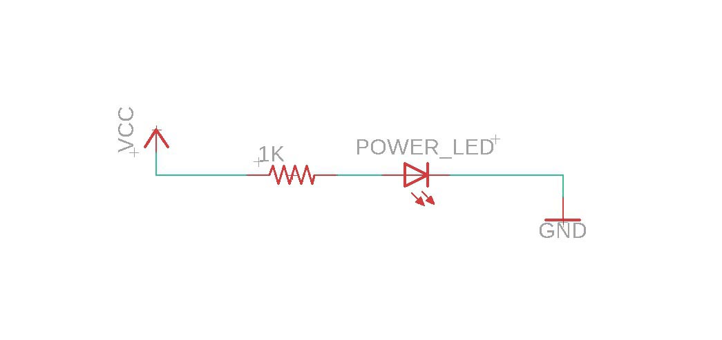
> Adding a Power LED
I wanted to add a power LED to my board because I wanted to have a visual representation of it if it was getting power or not. I didn’t want it to be super bright, so I just added a 1k Resistor in series with it. Here’s the Schematic for that.
> Adding the Two Programmable LEDs
For the two Programmable LEDs, I connected their ground pin to GND, and the positive terminal went to a Microcontoller input through a 1k resistor.
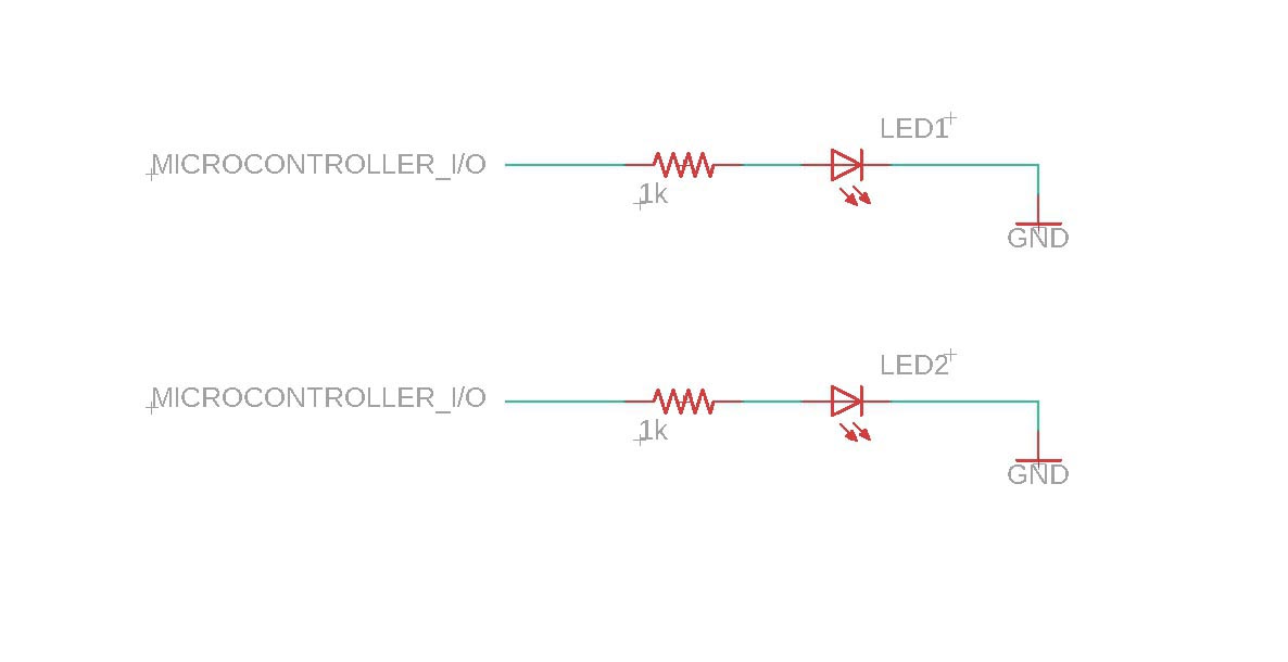
After Planning out my Circuit, I went on to design everything on a Circuit Design Software.
4. Software Selection
For the Electronics Design software, I had multiple options. I have some experience working with Proteus and Eagle as my previous workplace used them quite extensively. There was KiCAD , EasyEDA , tinkerCAD which all had their own perks.
5. Eagle CAD
EAGLE is a scriptable electronic design automation application with schematic capture, printed circuit board layout, auto-router and computer-aided manufacturing features. EAGLE stands for Easily Applicable Graphical Layout Editor.
It is now a part Autodesk which has added features where I can directly link my circuits with my Fusion360 work. I will be using Eagle 9.31 with an Educational License for the Fab Academy Course.

Why Eagle?
I decided to choose between KiCAD and Eagle and chose Eagle after trying out KiCAD for a bit. I realized that KiCAD had a steeper learning curve and since I was already proficient with eagle, I didn’t want to waste any time and get to work.
Here are the main perks for eagle:
- Cross-platform — EAGLE can run on anything: Windows, Mac, even Linux. This is a feature not too many other PCB design softwares can boast.
- Lightweight — EAGLE is about as svelte as PCB design software gets. It requires anywhere from 50-200MB of disk space (compared to the 10+GB more advanced tools might require). The installer is about 25MB. So you can go from download to install to making a PCB in minutes.
- Free/Low-Cost — The freeware version of EAGLE provides enough utility to design almost any PCB in the SparkFun catalog. An upgrade to the next license tier (if you want to make a profit off your design) costs at least two orders of magnitude less than most high-end tools.
- Community support — For those reasons, and others, EAGLE has become one of the go-to tools for PCB design in the hobbyist community. Whether you want to study the design of an Arduino board or import a popular sensor into your design, somebody has probably already made it in EAGLE and shared it.
Eagle Workflow
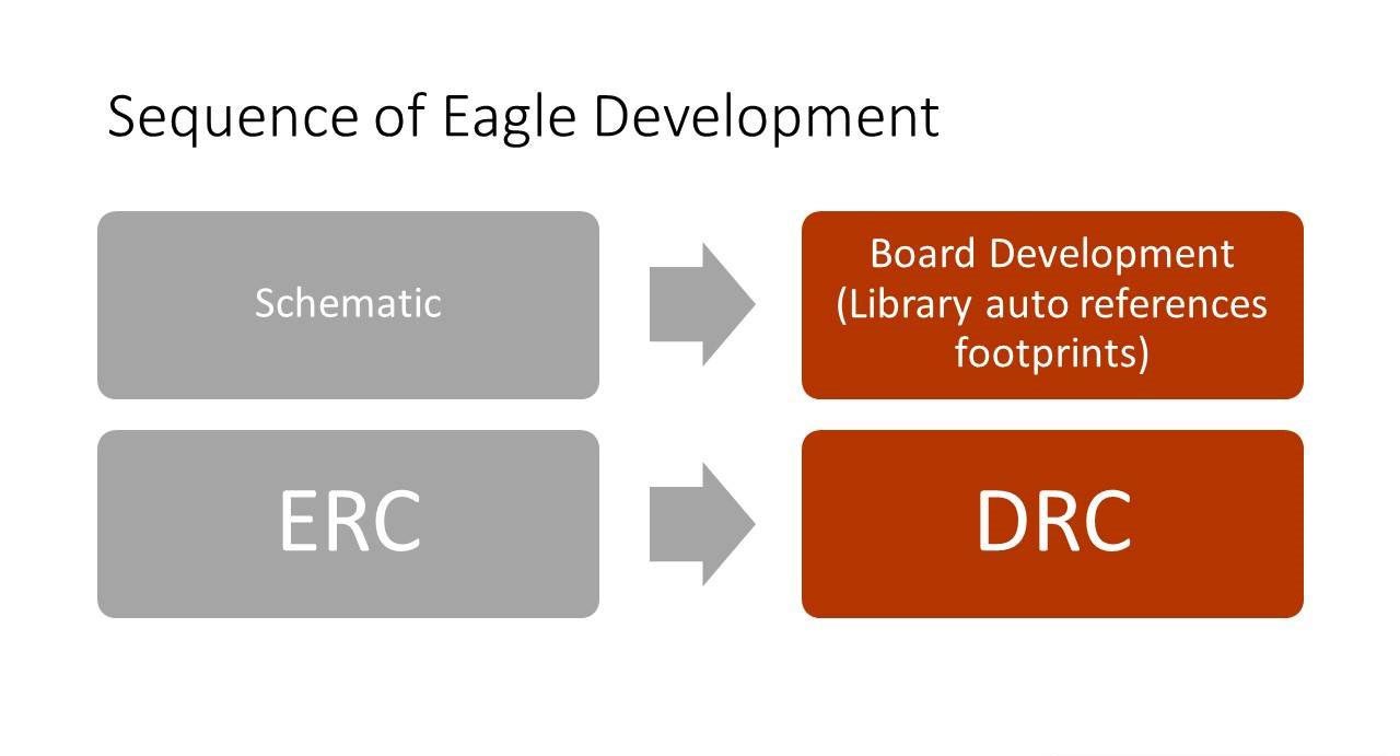
The Eagle workflow consists of two main sections.
- The Schematic Design, which is governed by the ERC(Electrical Rule Check)
- The Board Design, which is governed by the DRC(Design Rule Check)
Links
Installing Eagle
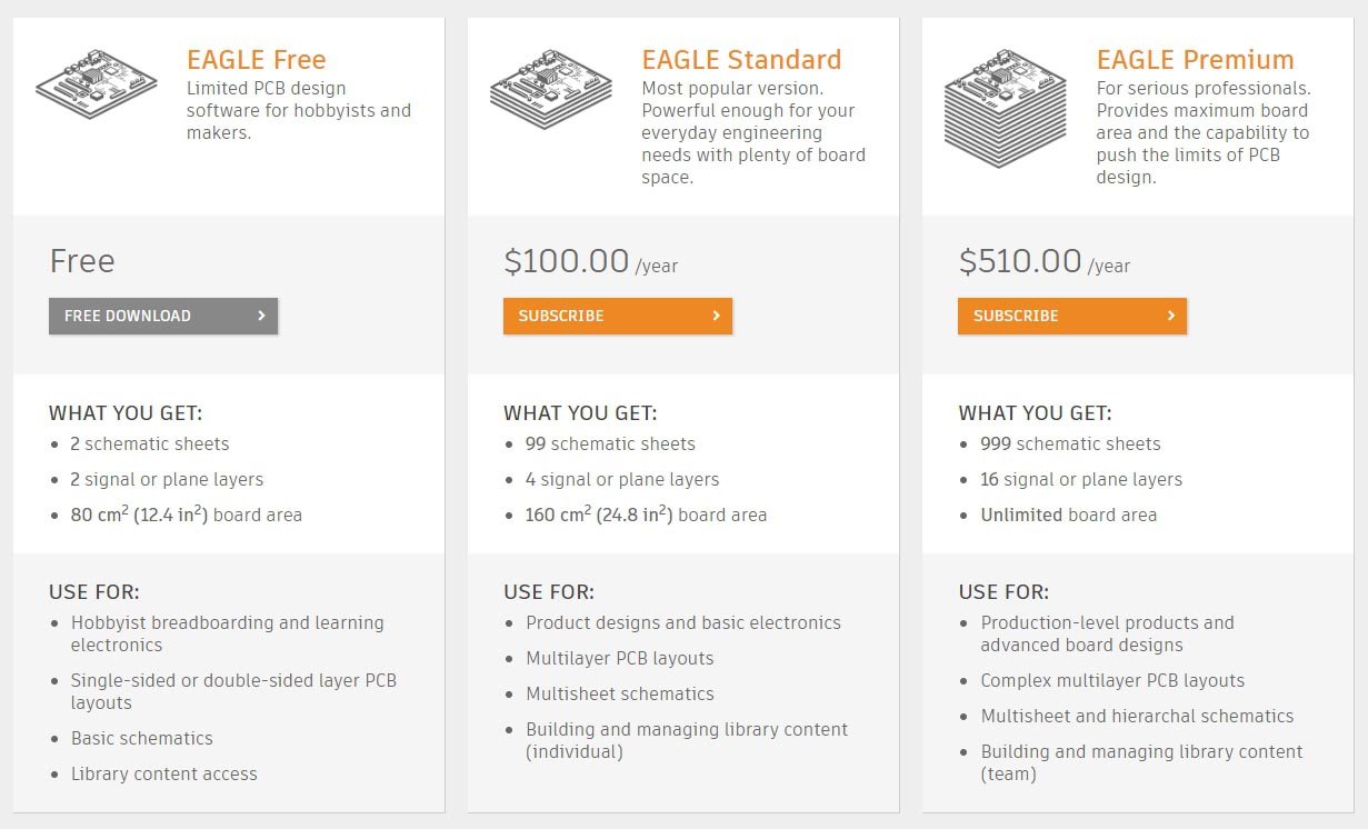
Eagle is not a free Circuit Design Software. But there is a free version available for Hobbyists and Students. There is a Standard version which is available for everyday engineering and then there’s the premium version which can be used for production level PCB designs. This illustration shows a comparison of all the versions.
I will be using the free version of Eagle as it gets all my work done without any issues. It can be downloaded for multiple platforms from
Links
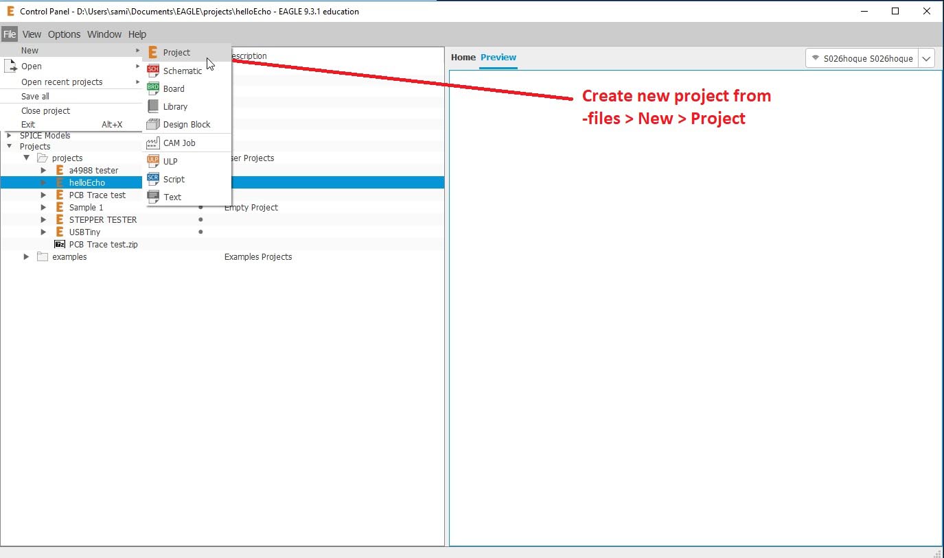
Creating a Project
Making a Schematic
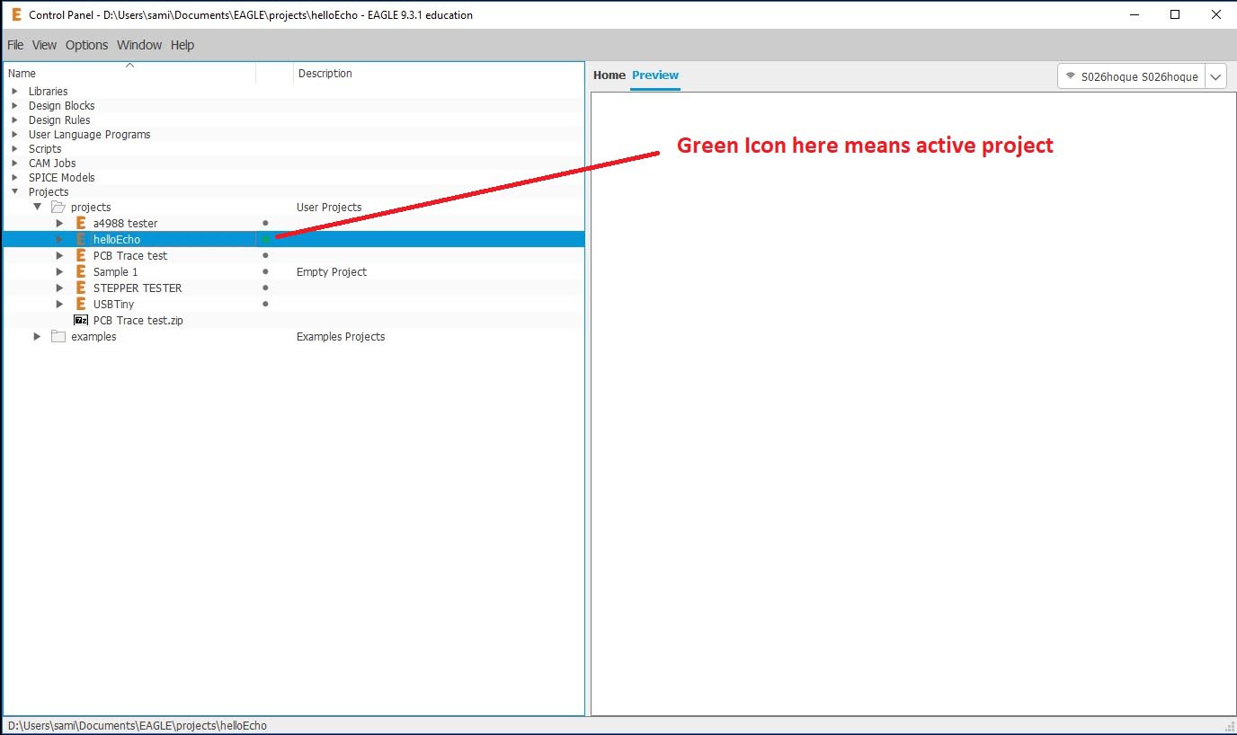
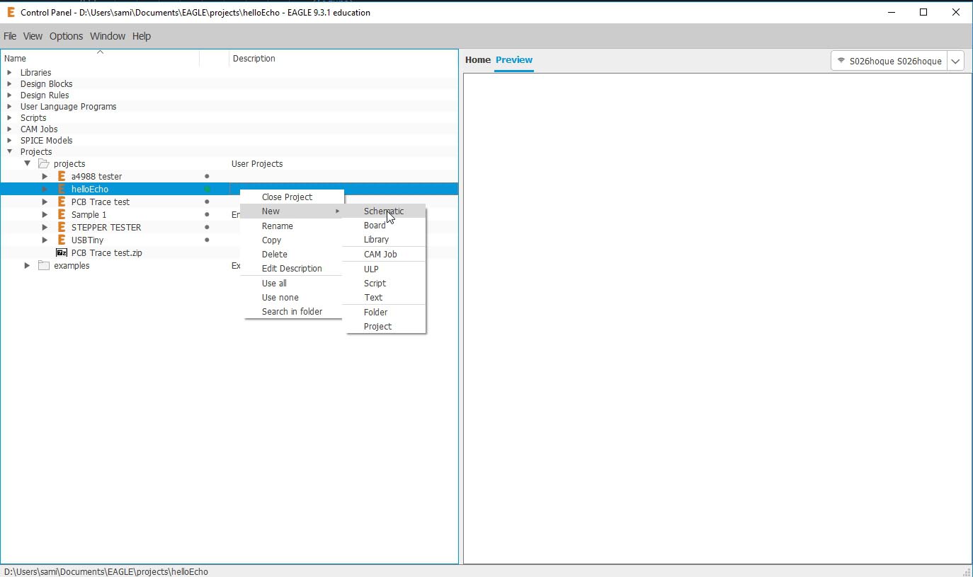
First We have to create a schematic file by right clicking on the active project, and creating a schematic. We can start editing the schematic by double clicking on it.
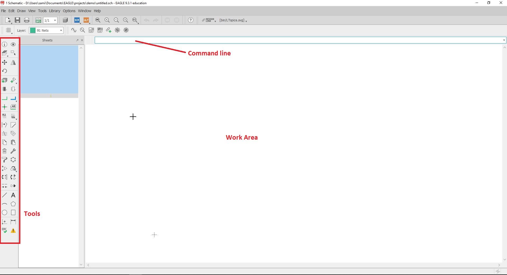
This is how the Schematic Editor Window Looks like
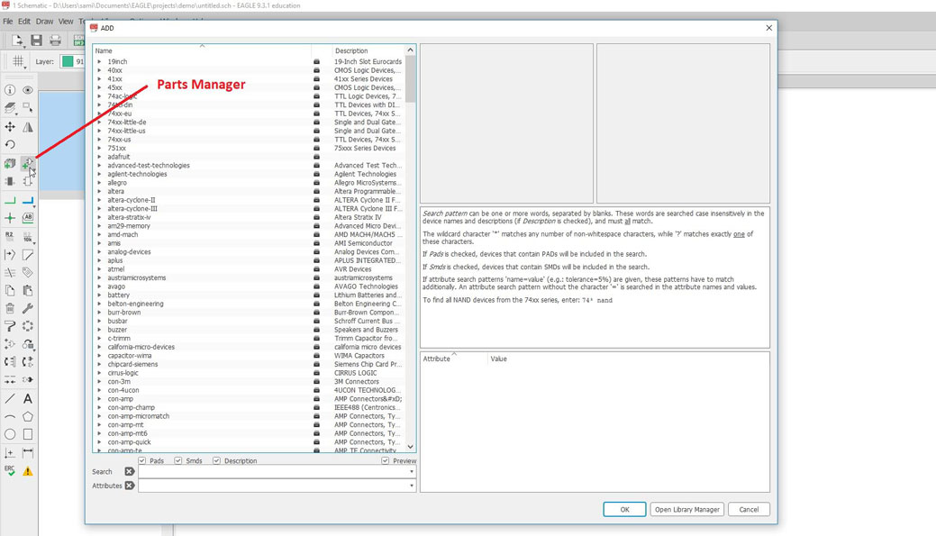
Picking Components
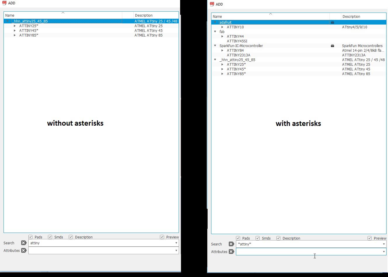
Installing the Fab Library
Library Manager
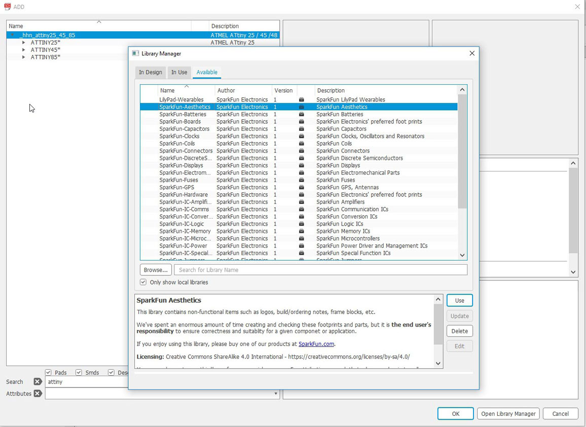
You can bring up the library manager from the parts manager menu. Eagle 9.3 has the option of adding managed libraries here from the ‘available’ tab. You can automatically install and keep your libraries updated from here.
Adding Custom Libraries
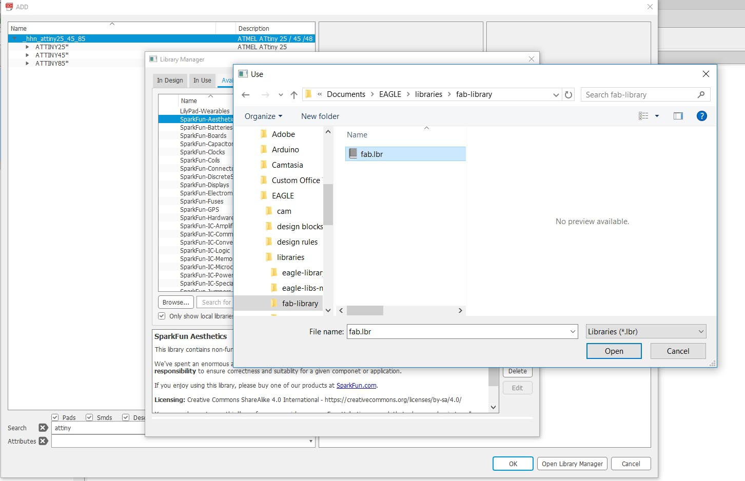
For custom library you just have to download the library and use the browse option in the library manager to open it. The Fab Library can be downloaded from here.
Connecting Wires
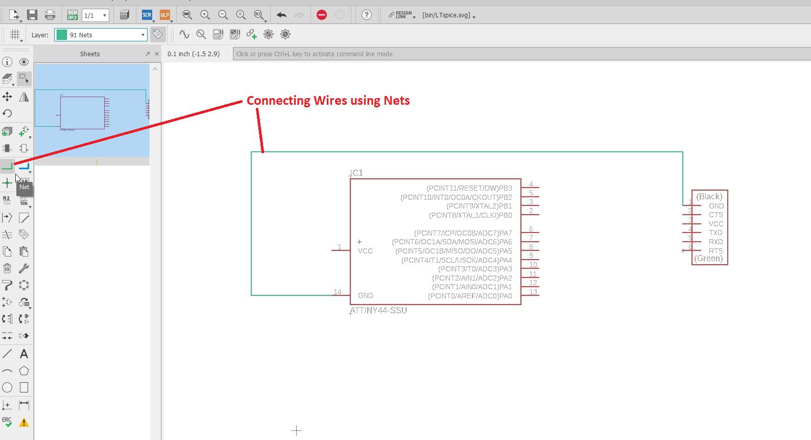
Wires can be connected directly using Nets.
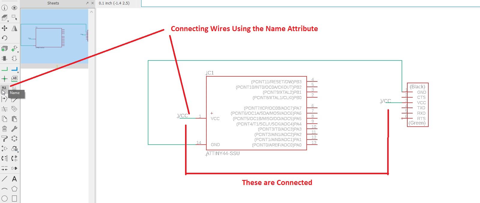
They can also be connected using the name attribute.
Checking for errors: ERC
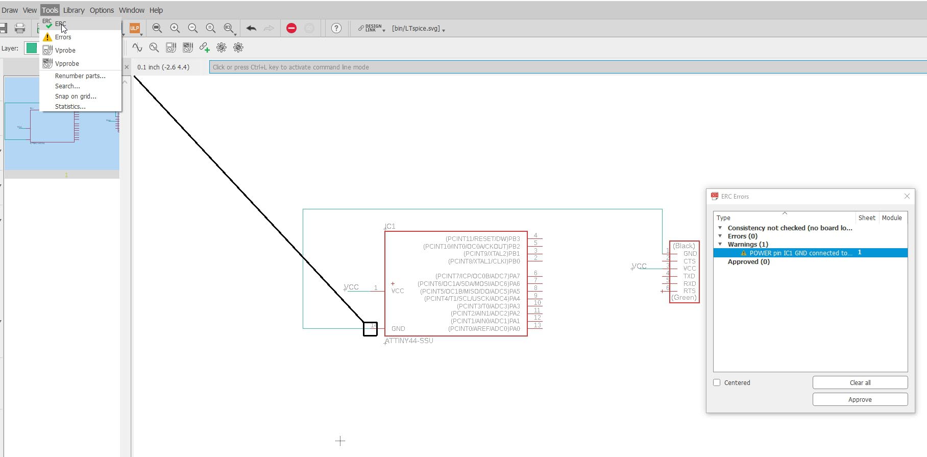
The ERC is a tool to check for errors in a schematic. It can be found under the tools menu. As for example here, ERC is warning me that the GND of IC1 is connected to n$1, which is the name for the GND pin of the FTDI connector. It is just a warning to show if I want to approve of this connection or not.
Creating a board file from a schematic
After placing all the components I required, I was ready with my schematic.
After placing all the components I required, I was ready with my schematic.
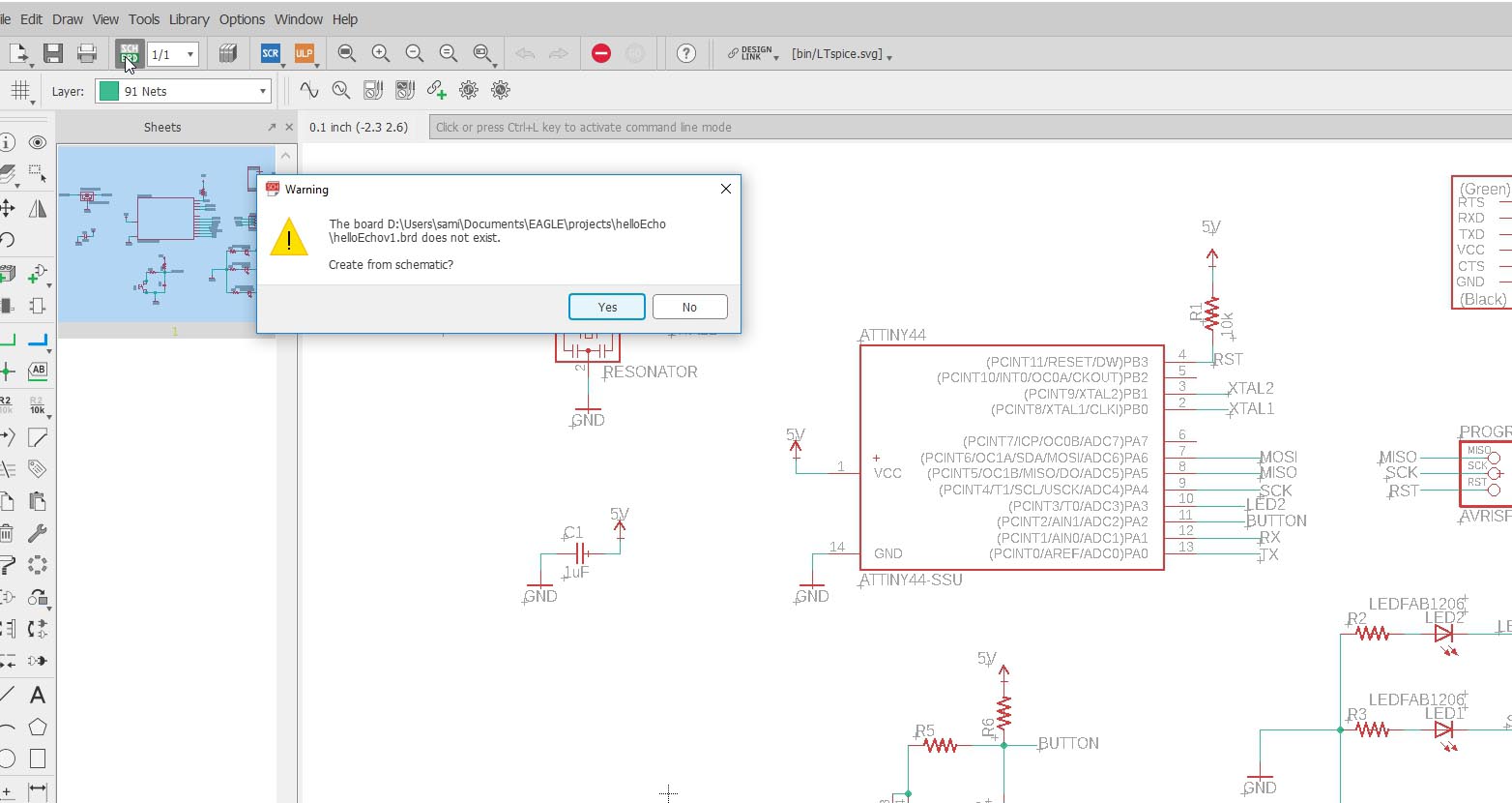
To Create the board file, I just clicked on the brd icon on top and Eagle automatically generated it for me.
*Note that You have to keep both your board and schematic window open.
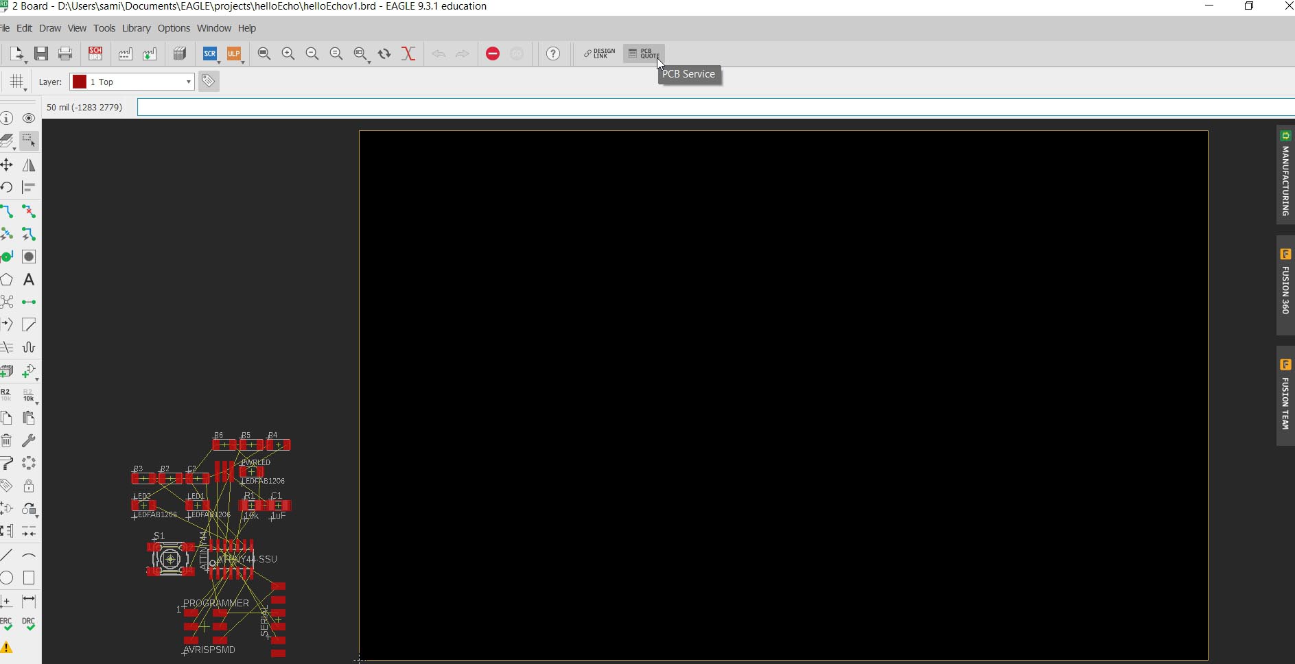
Placing Components in a board layout
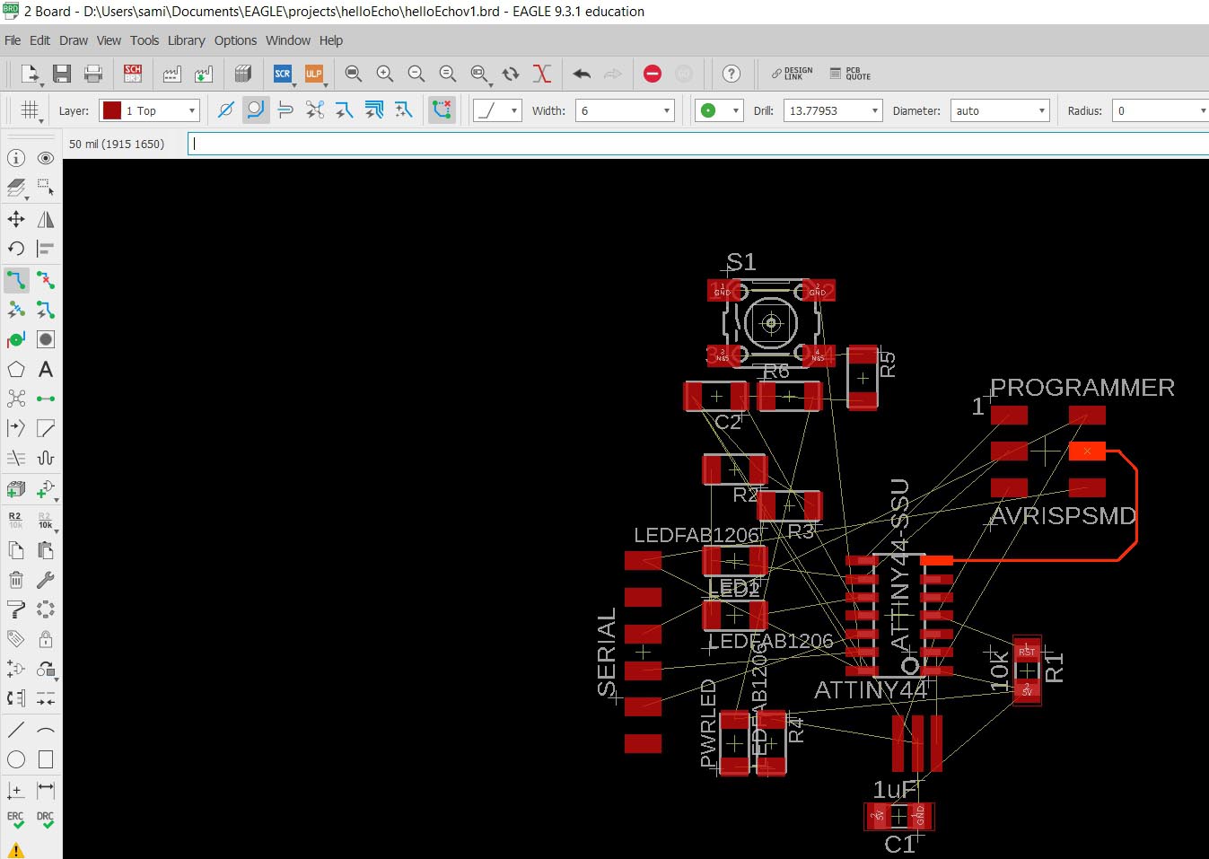
Now that I had my schematic prepared, and board file generated. I started to place my components in a layout where I could connect all the wires without overlapping any of them. I first started with a general layout, without much detail to the distancing,
DRC, Design Rule Check
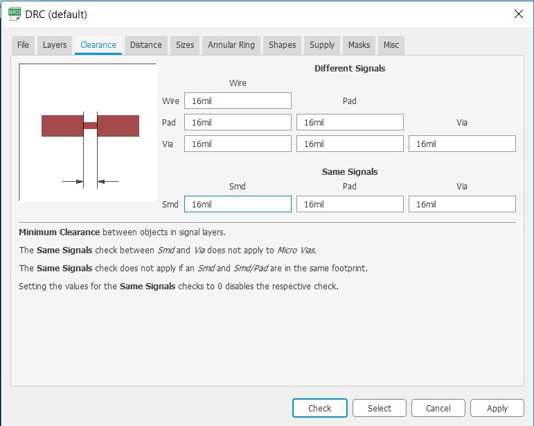
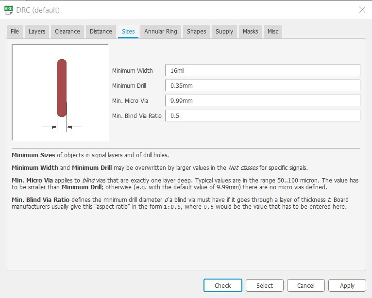
The DRC is the tool that governs our PCB design. It can be brought up from tools > DRC. The minimum Trace width, the minimum distances between various components can all be configured here, and if we break any of the rules during the design process, DRC will help us resolve those.
My DRC rules were the following;
Clearances:- 16 mil on everything
Sizes:- Minimum Width: 16mil
- Minimum Drill: 0.8 mm
Manual Routing
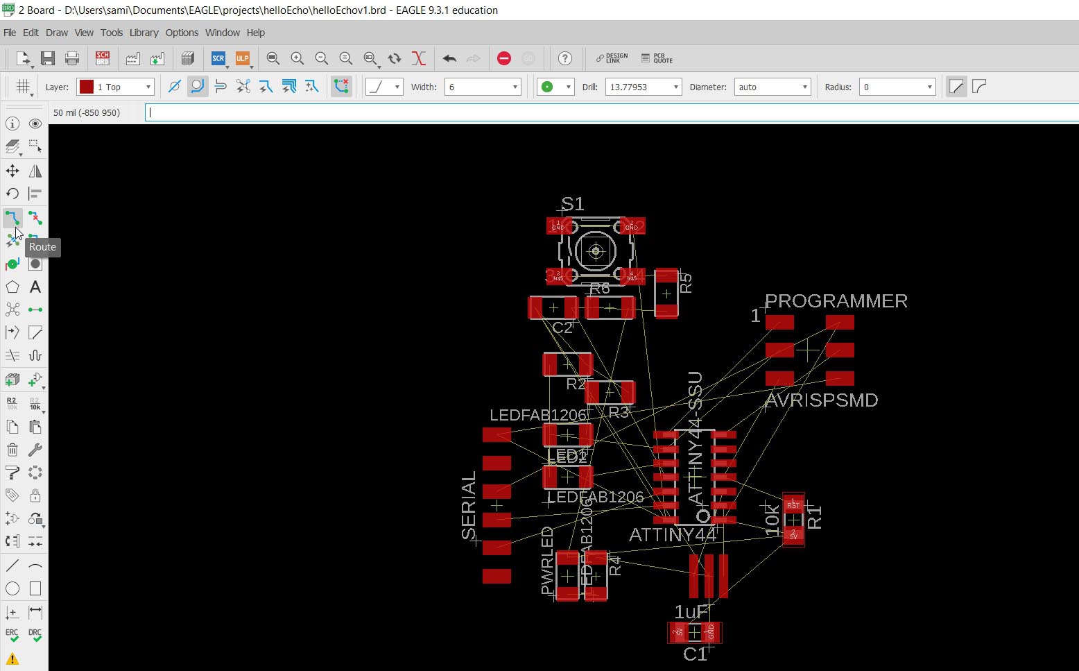
Routing Can be done by clicking on the route tool, the pads that need to be connected are highlighted in red.
Auto-Router
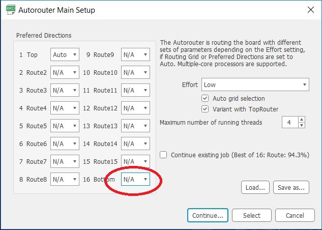
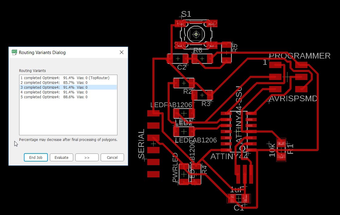
The Autorouter is a handy tool which helped me route my PCB. It can be found under the tools menu. Make sure to check the bottom layer as N/A before starting to autoroute. The Autorouter will follow the DRC and try to connect all of your traces. It will help you find closed loops where you need to do manual routing or change the orientation of components to optimize your routing.
The Meander Tool
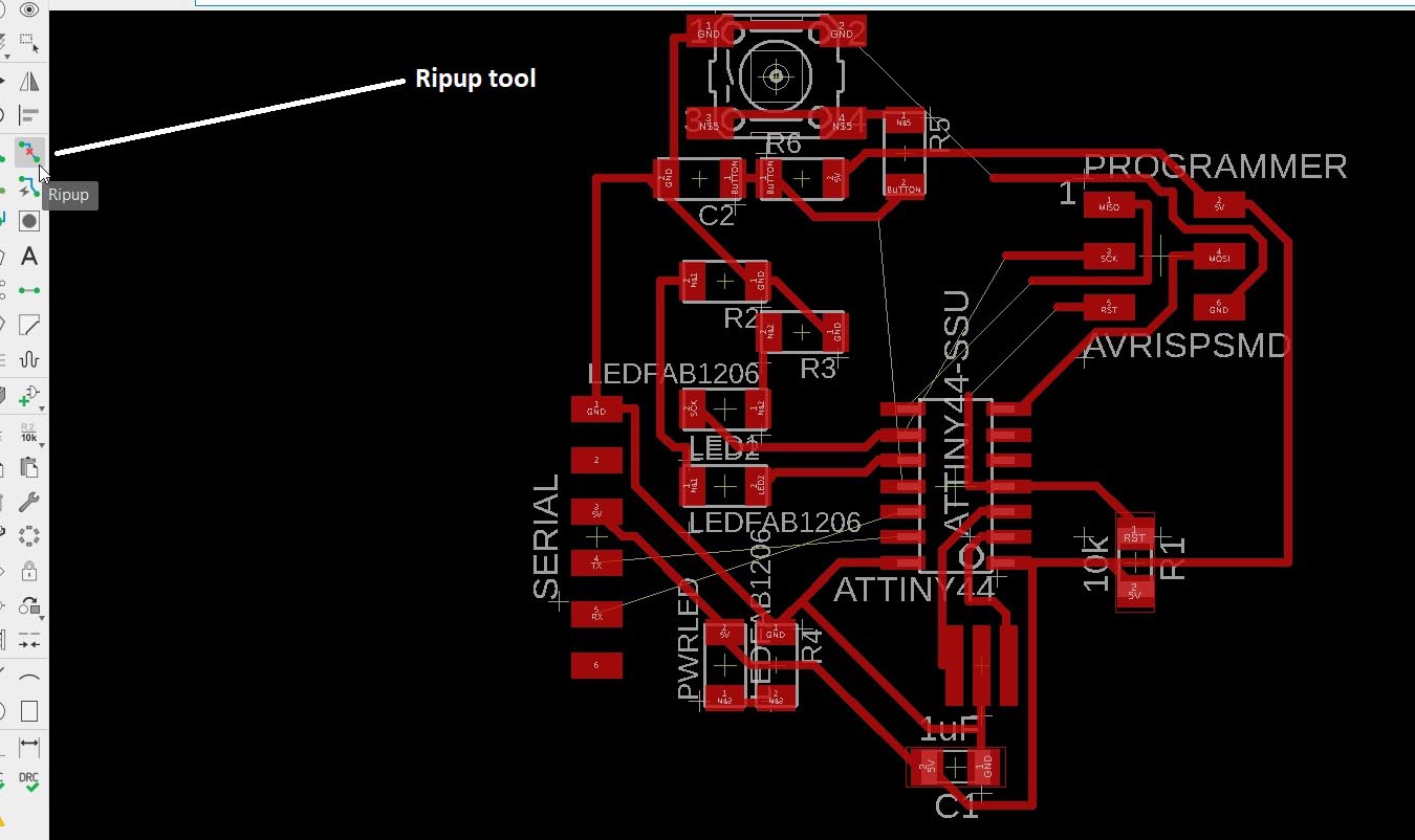
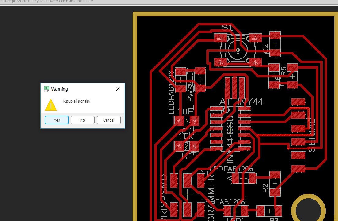
Now if you are not satisfied with your autorouting, or if you want to delete any of your routing, you have to use the meander tool. For removing all traces, the command ‘RIPUP;’ needs to be used.
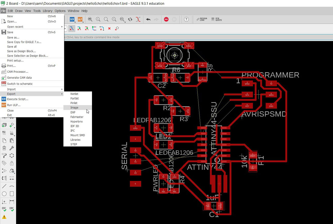
Exporting your PCB
Eagle has many Export options, but none of them are quite refined. You have to do manual graphics manipulation to get a workable PNG file from a design. For that I started to explore a bit into Eagle Automation Scripts to find a lazier way to export PCBs
Eagle Automation Script
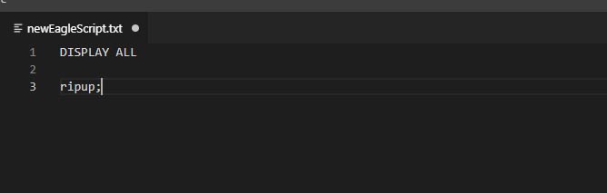
Eagle scripts are text files with eagle commands. You can use them for automating tasts such as changing the width of all traces on a board, changing board size or drawing specific pattern.
How to use Eagle Scripts
- Simply create a text file and open with your preferred text editor, I am using Visual Studio Code.
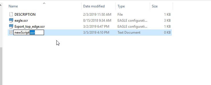
- Write your script and save your file. After you’re done, just change the extension to .scr
- Save this file on your Eagle User directory, for windows users, it is usually at
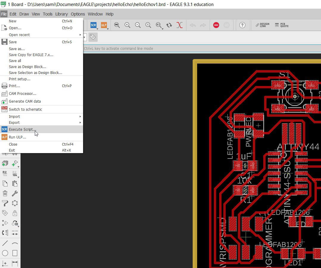
/Documents/Eagle/Scripts - Click on File, Execute Script, Browse to your script to run it.
More on Eagle Scripts
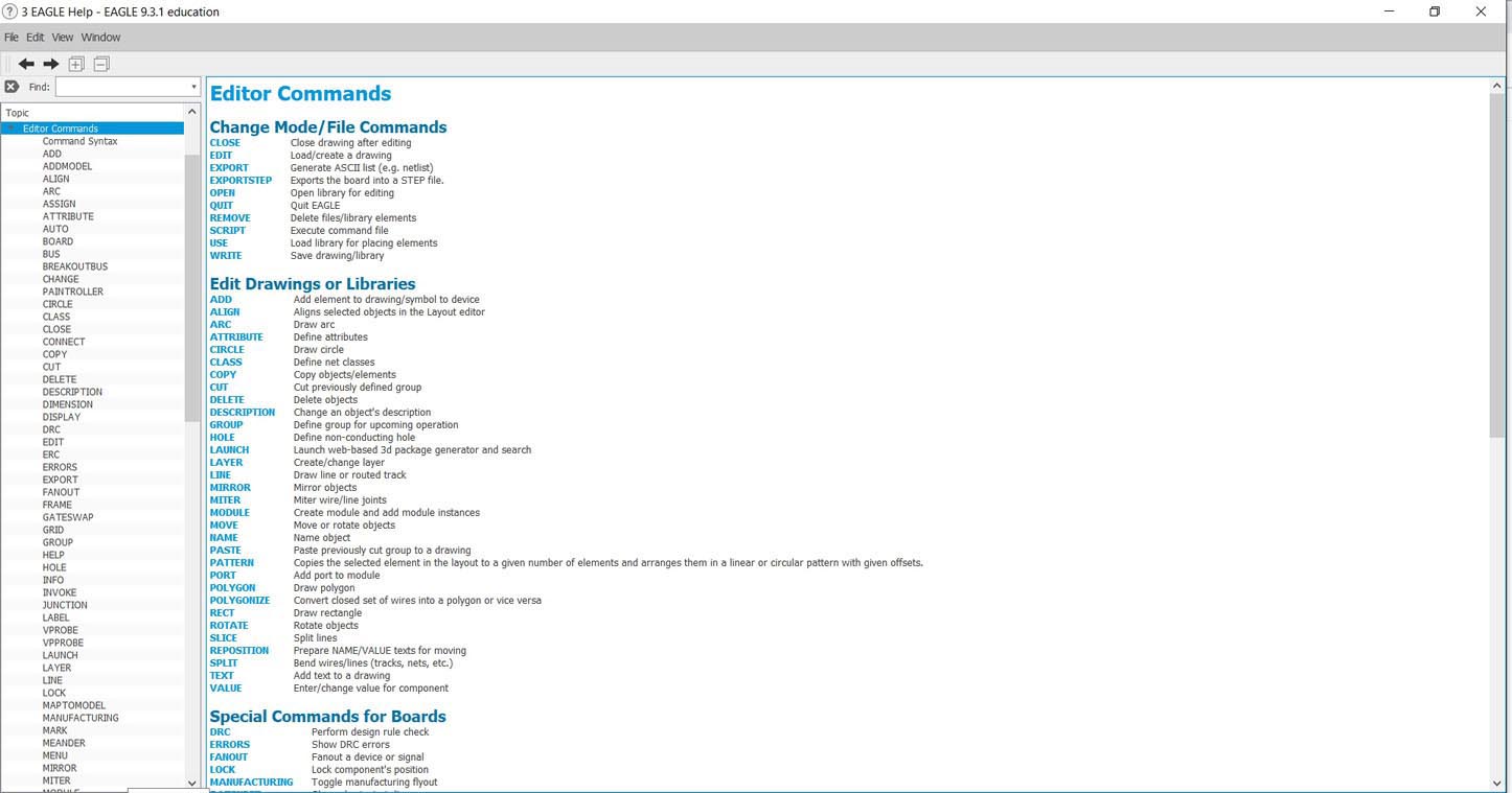
More info on Eagle Scripts can be found in Eagle’s built in Documentation. Click on Help>General Help> Editor Commands
Links
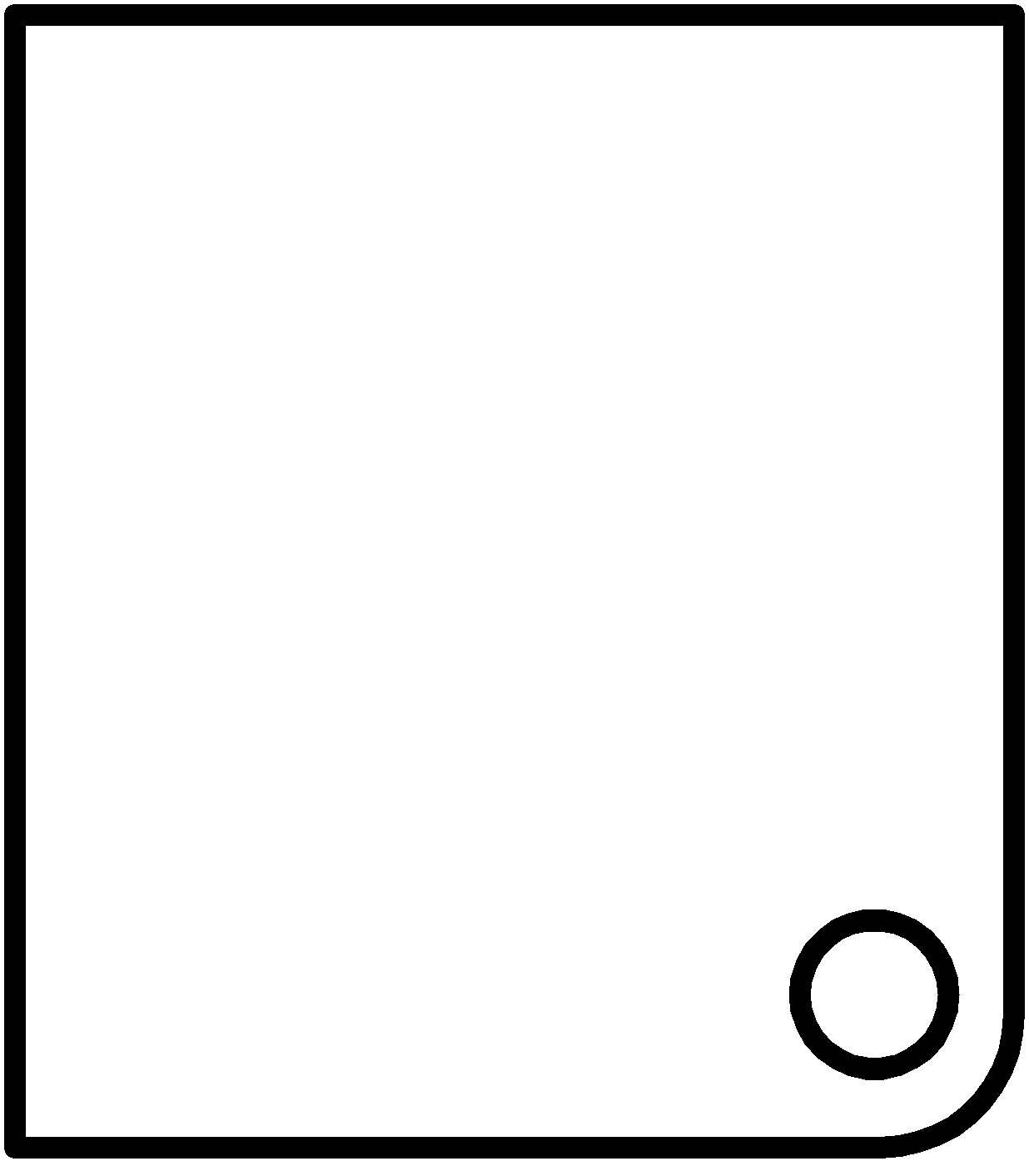
The One Click PCB export Script
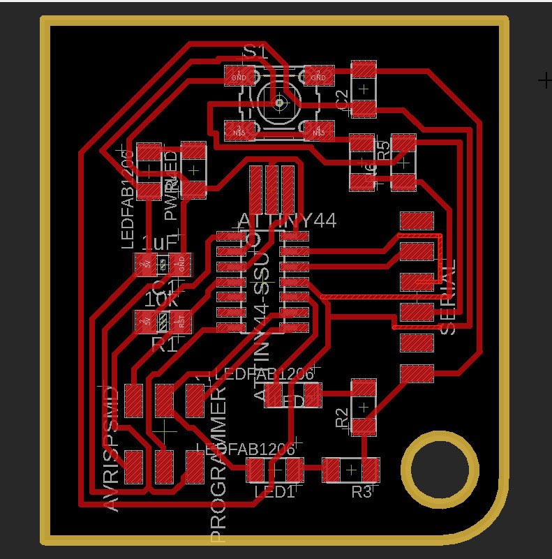
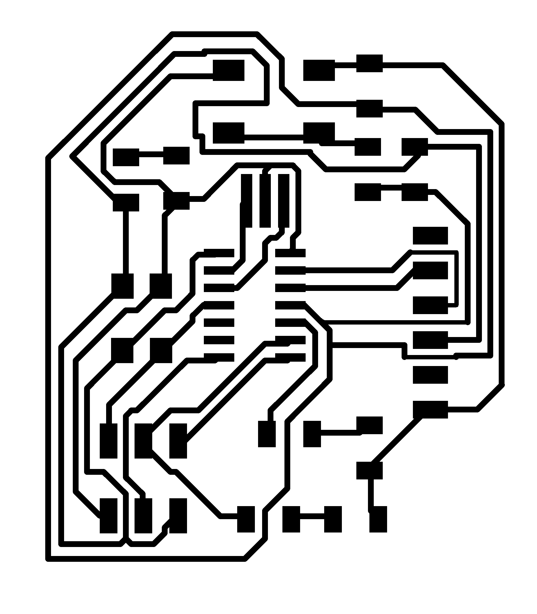
After a bit of experimenting, I wrote a one click method to export PCBs from Eagle. This script works for single layer layer boards with the board border drawn on the Dimension layer. Change the directory of your exports accordingly and it should work.
DISPLAY ALL RATSNEST DISPLAY None DISPLAY Top Pads set palette white; EXPORT IMAGE D:\pcb_top.png MONOCHROME 1200; DISPLAY None DISPLAY Dimension EXPORT IMAGE D:\pcb_bottom.png MONOCHROME 800; DISPLAY ALL set palette black;
Script Output
Links
My eagle project folder can be downloaded from here. HelloEcho.zip
6. Milling
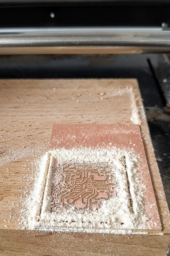
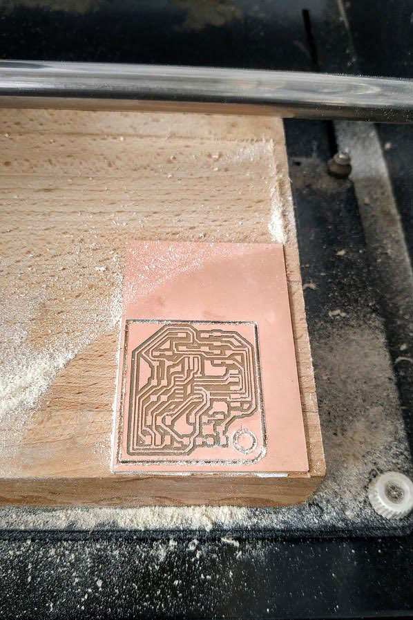
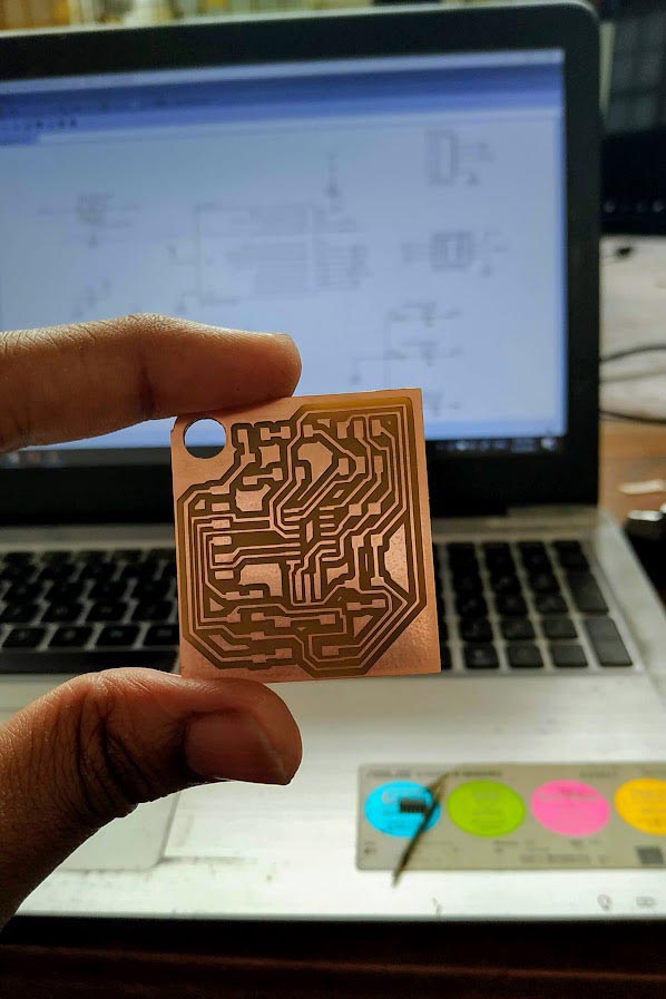
I used our trusty old MDX-20 to mill out our board. I used Fab modules to generate the toolpath and to send it to the machine. More documentation found on milling can be found on my Electronics production week, specifically here .
The settings I used to mill this board were as follows:
Traces (1/64)
- cut speed: 4
- cut depth(mm): 0.1
- tool diameter(mm): 0.4
- number of offsets: 4 [This is the number of offset cuts there will be outside the copper trace, increase this to remove more excess copper. -1 will remove copper from the board completely except the traces.]- offset overlap(%): 50
- path error(pixels): 1.1
Outlines (1/32)
And these are the Settings for PCB outlines,
- cut speed: 4
- cut depth(mm): 0.6
- Stock Thickness(mm): 1.7
- tool diameter(mm): 0.79
- number of offsets: 1
- offset overlap(%): 50
- path error(pixels): 1.1
- image threshhold: .5
7. Component Collection
I like to collect my SMD components in masking tape. It makes it easier to collect and document as well. For this board, I made my parts list and went on to collecting the components.
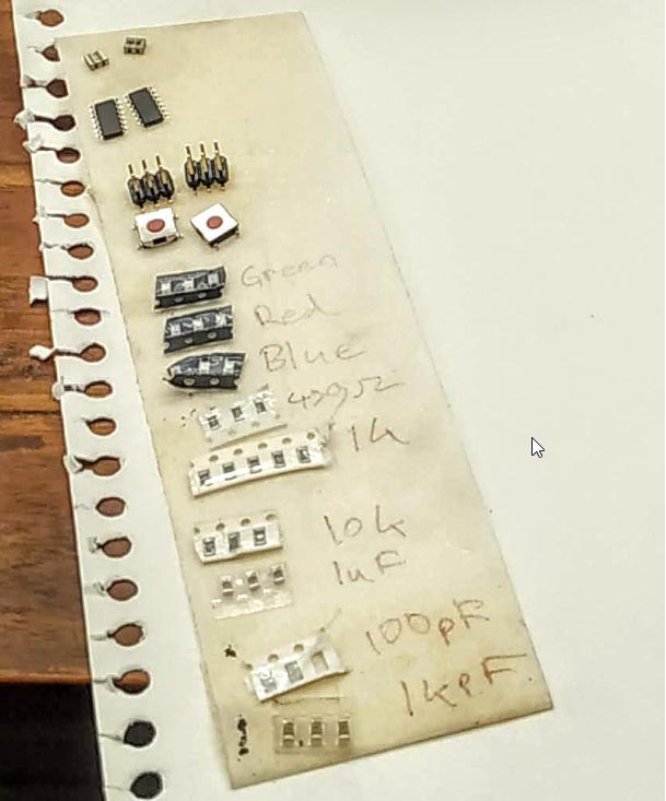
| Name | Quantity |
| ATTINY44 | x1 |
| Resonator 20Mhz | x1 |
| 1uF ceramic capacitor | x1 |
| 0.1uF ceramic capacitor | x1 |
| 10k Resistor | x2 |
| 1k Resistor | x4 |
| Red 1206 LED | x1 |
| Green 1206 LED | x1 |
| Blue 1206 LED | x1 |
| 6Pin Double headers for ISP | x1 |
| 6Pin FTDI Connector | x1 |
8. Soldering
With my component collection done, I was ready to solder. I prepared with all the necessary tools and it took about 30 minutes to solder the whole board.
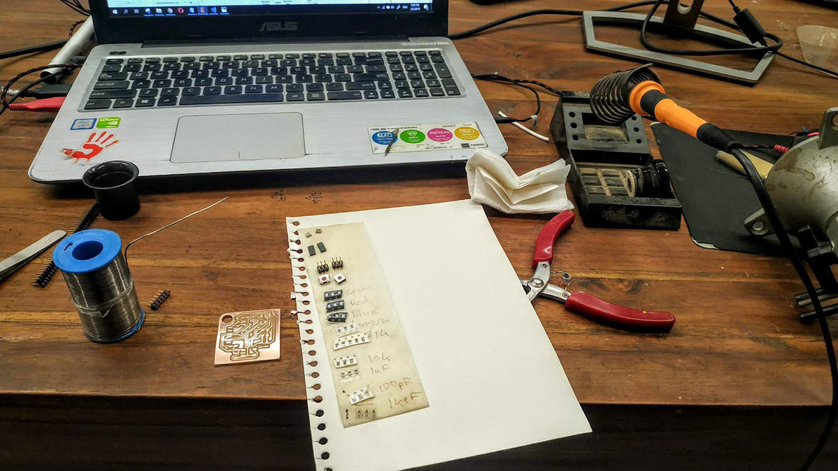
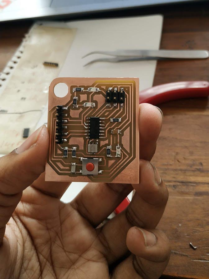
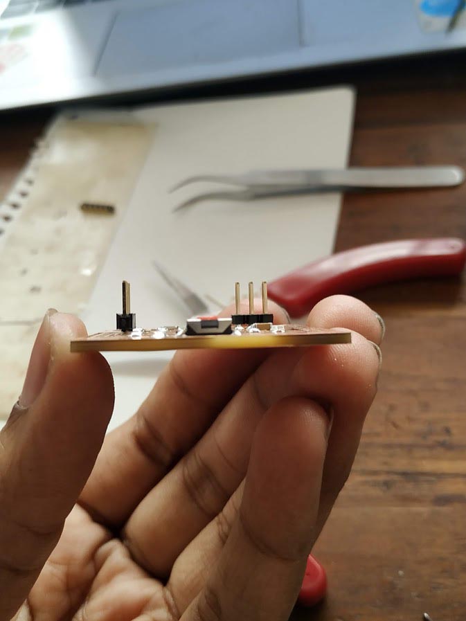
9. Programming
To program the board I will be using the Arduino IDE and my FABISP to upload it. I will be powering my circuit using an FTDI Module as a power source.
Installing Arduino
Arduino can be downloaded free from the official website here. Installing it is very straight forward.
Adding TinyCore (support for ATTiny MCU Series to Arduino)
To program the ATTINY microcontroller family using Arduino, I will be using ATTinyCore, which is an Arduino core for ATtiny 1634, 828, x313, x4, x41, x5, x61, x7 and x8 series of microntrollers. The installation instructions are given on the github page and I just followed the Instructions for the Boards Manager Installation Method.
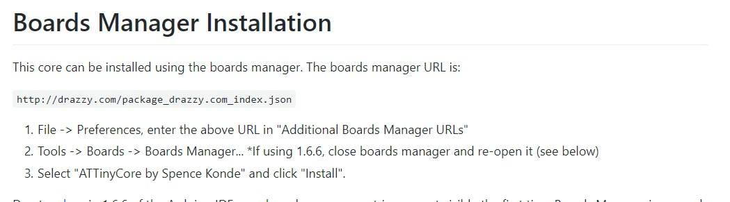
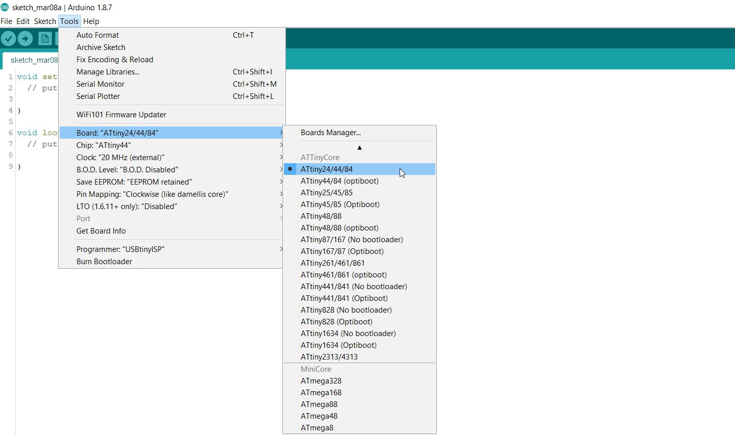
If all went right, your arduino should have the ATTiny Core listed on your boards list.
Uploading a Blink Code
I used a cheap chinese FTDI module to supply power to my HelloEcho Board, which in turn supplied power to my FABISP. So the connection was like this,
- the ISP programmer header on my HelloEcho board was connected to the ISP programmer header on the FABISP.
- The 5v and GND from my HelloEcho board was connected to the 5v and GND of the FTDI cable.
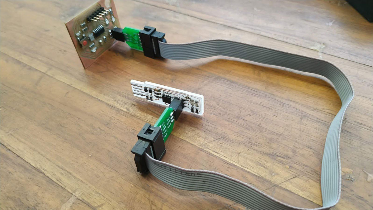
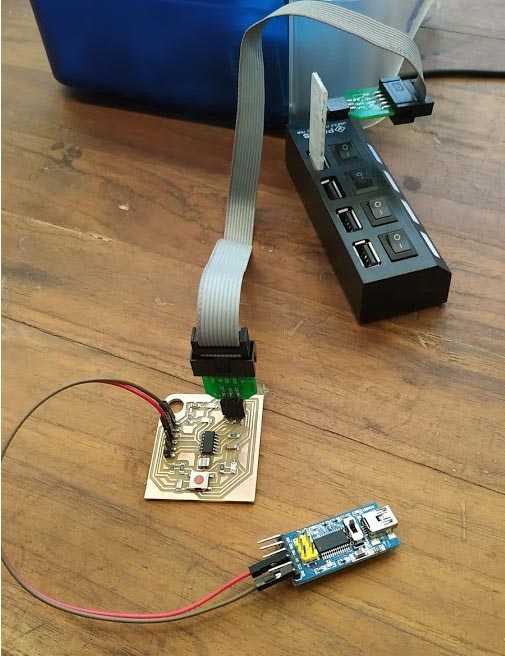
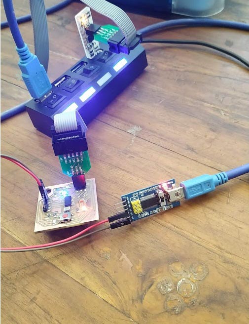
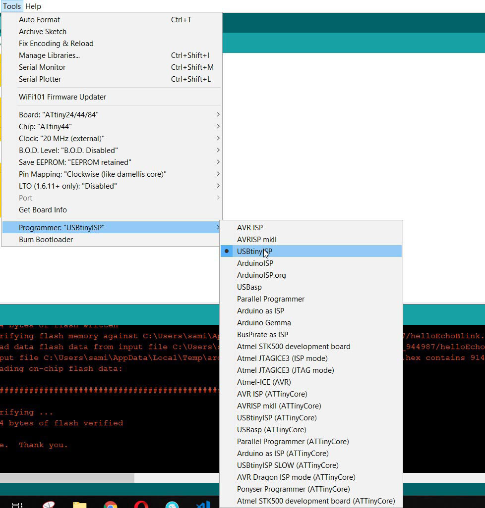
Here are the settings I used on arduino to upload the code.
- Board: ATtiny24/44/84
- Chip: ATtiny44
- Clock: 20MHz (external)
- Programmer: USBTInyISP
Everything else was on default.
Then I wrote this code, and uploaded it. Download Code
Adding more LEDs to the mix
Then I tried blinking the other LED as well. But with a different delay.
Output:
Pushbutton Code
On this code, I added the a pushbutton input as a logic to blink different LEDs.
Output:
10. Diffuclties Faced
Ripped out FTDI Connector
I ripped off my FTDI connector on my first board during plugging out the FTDI connector. I used a different FTDI module later to upload my code from which I only took the 5v and GND.
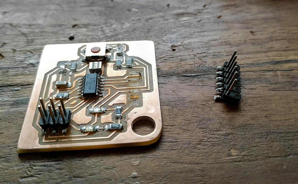
11. Learning Outcomes
Since I already had some experience with electronics, I got the chance to explore much further into Eagle.
- I learnt about Eagle automation Scripts and ULP and made a one click script to export PCBs as PNG files.
- I learnt why Brian’s FabISP had a power isolation on the programming pins, and I used an FTDI cable to supply power to my whole circuit.
- I learnt how to make modular Eagle Schematics, which came in handy later during my board design.
12. Hero Shots
Downloads:
Neil’s Hello Echo Firmware
My One Click Image Export Script
My eagle Project:
Test Code 1: Blinking 1 LED
Test Code 2: Blinking 2 LEDs
Test Code 3: Pushbutton+LEDs blinking
Learning Outcomes
- I explored how Neil Wrote his hello echo firmware in C
- I already knew how to use eagle, I just explored a bit into the new library manager of Eagle.
- I used my Fab ISP to program my helloEcho boards, both of them worked on the first go.
What I need to explore:
- I need to learn kiCAD. I didn’t have much time this week, so I couldn’t explore much of it.